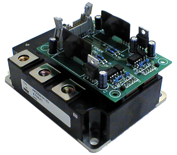
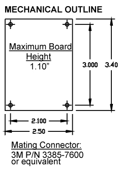
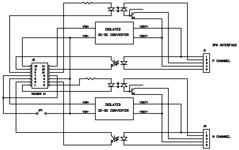
The AP-1174 provides a complete, field-tested turnkey solution to drive a single large area thyristor device. This driver accepts a logic level control input and provides an isolated DC drive current into the SCR gate, able to hard drive up to 100mm size devices. The output gate drive signal is applied thru a pulse forming network that creates a fast rising leading edge current pulse (typically 5A/µSec) into the SCR gate, maximizing the device di/dt capability and insuring proper SCR turn on. The on board 115VAC power supply provides all needed power to drive the SCR and provides transformer isolation between the AC input and the SCR being driven. A high speed optocoupler provides isolation between the customer supplied logic level signal and the SCR. LED indicators display POWER ON and SCR ON status. The small footprint PCB assembly measures only 3.0” X 5.0”. The AP-1174 provides a complete, tested, fast time-to-market solution for customers who need to interface to POWEREX V-Series Dual IPM modules. The AP-1174 incorporates two isolated DC-DC converters which supply power to the IPM module. High speed optocouplers provide the proper interface between the module and the customers’ control electronics. The assembly provides direct mounting to the IPM module and is packaged in a small footprint printed circuit board that measures only 2.50” X 3.40”. The AP-1174 supports the following IPM modules:
|
click images and diagrams to enlarge |
|
||||||||||||||||||||||||||||||||||||||||||||||||
|
||||||||||||||||||||||||||||||||||||||||||||||||
|
||||||||||||||||||||||||||||||||||||||||||||||||


