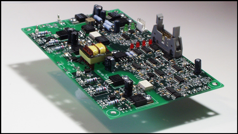
FEATURES INCLUDE The BAP-1551 Insulated Gate Bipolar Transistor (IGBT) Gate Drive Board (GDB) discussed in this Datasheet/Applications Note provides a safe, reliable, isolated interface between control logic and an IGBT based power stage. With minimal development time and cost, a single phase half bridge inverter, with up to three dual IGBTs in parallel, can be designed and built using the techniques described below. Two half bridge inverters can be configured as a full bridge and three half bridges can be combined to create a three phase system. |
click images and diagrams to enlarge |
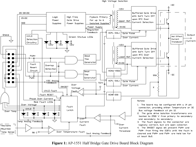
Typically, the most unreliable portion of a motor controller/inverter design is the power stage. In most if not all cases, this is due to inadequate control of the power semiconductors. The APS IGBT GDB is a robust design (see Figure 1 Block diagram) offering the necessary protection features to ensure a reliable power stage including: two forms of over current protection, DC link over voltage protection, over temperature protection, and under voltage lock-out. Also provided as feedback signals to the control logic are isolated, analog, real-time representations of the output current, the DC link voltage and the temperature sensor interface that can be mounted on a heatsink.
GDB Power Supply
The BAP-1551 GDB requires either an unregulated 24 volt (20-30) or regulated 15 volt (14.5-15.5) power supply to operate (see Table 1 for pin assignments). The system designer must choose one supply or the other, whichever is available or preferred. Note: Connecting both power supplies simultaneously will create contention issues that may result in damage to the board.
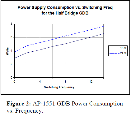
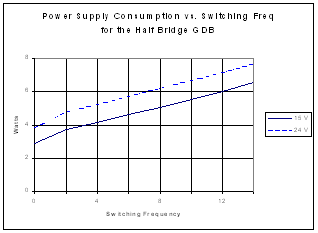
The input voltage is used to generate the logic control power supplies and the isolated bipolar power supplies for the upper and lower IGBTs. The power consumed by the 24-volt or 15-volt supply is proportional to the gate charge and the switching frequency of the IGBT being driven. The larger the IGBT in a particular manufacturer’s series, the larger the gate charge, therefore the more power it will consume.
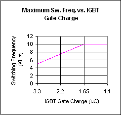
Figure 2 below is a graph of estimated power consumption vs. switching frequency for a half bridge configuration employing three dual IGBTs in parallel, each with a gate charge of 1100hC. The value at 0Hz is the power consumed by the GDB before switching IGBTs of any current rating. The power consumed increases with switching frequency and is proportional to gate charge. To determine the power required for a specific application, look up the gate charge (usually given in ?C on the data sheets of the selected IGBT) and offset the power consumed by the GDB at 0 Hz by the power consumed by switching IGBTs. Note: It is not recommended to run three dual IGBTs in parallel, with a gate charge of 1500hC or more, beyond 20KHz. Excessive heating of gate drive transistors may occur, resulting in potential damage to the board.
Control Signals
The user provided control signals that determine the IGBT conduction state require 0 volts for an OFF command and 15 volts for an ON command. These signals are referenced to the GDB power supply ground and are labeled PWM+ for upper IGBTs and PWM- for lower IGBTs on connector J1 (pin assignments located in Table 1). These signals are fed through Schmitt-triggered buffers to ensure fast edges for the overlap detection and dead time generation circuitry.
The overlap detection circuitry inhibits the upper and lower IGBTs from firing simultaneously, which would result in a potentially destructive shoot through current. If an overlap is detected, both the upper and lower IGBTs are held off until one of the IGBT control inputs (PWM+ or PWM-) go low, at which point the compliment will turn on.
Dead time, is the delay from when the user provided control signal goes high to when the on signal is applied to the gate of the IGBT, is generated on board. Therefore, dead time is neither required nor desired on the incoming control signals. User provided dead time may effect the RESET function described in the Protection Features section below. Standard dead time is set to approximately 2ms. Consult factory for alternate dead time settings.
To ensure optimum current sharing of paralleled IGBTs during transients, the control signals are trifurcated after the optical isolation. Therefore, deviations in optical propagation delays will not impact dynamic current sharing.
Gate Drive Signals
After the control signals are integrated with dead time, they are optically isolated and buffered by a transistor stage with the capability to source and sink the high peak currents necessary to turn large IGBTs on and off quickly. The GDB is equipped with 4.3-Ohm gate resistors standard, which allows for up to 3 Amp peak current pulse. This resistor is selected to optimize the performance of an IGBT with a gate charge of approximately 1000hC; however, it will work in many applications. Consult the factory for alternate gate resistor values.
The isolated gate drive power supplies are generated with a high frequency transformer. This transformer is high potential tested to 2500 volts between each of its three windings. The primary of the transformer is referenced to the ground of the 24 volt or 15 volt power supply.
Each secondary is referenced to the emitters of up to three IGBTs in parallel. Although emitters of three IGBTs may be tied together, each will have a distinct emitter pad on the GDB to facilitate connection to an IGBT via a twisted pair. The capacitance between secondaries is less than 15 pF to minimize capacitive coupling between the upper and lower IGBTs.
Each secondary creates a bipolar power supply that is optimally regulated to sufficiently drive the IGBT into saturation yet low enough to limit short circuit currents and minimize power supply consumption. A negative bias is provided when the IGBT is off to ensure it remains off and to minimize turn off losses.
Current Sensing
The APS GDB is specifically designed to operate with open loop Hall effect sensors. The GDB provides the necessary ±15-volt power supplies and ground reference for three separate current sensors (see Figure 3). Isolated voltages proportional to each current sensor output are fed back to the GDB where they are summed, buffered and fed back to the user provided controller (see Table 1 for pin assignments) as a real time analog representation of the output current.
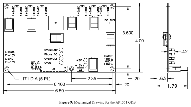
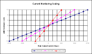
The gain of the signal conditioning circuitry on the GDB is set to unity with three dual IGBTs in parallel. Therefore, if the Hall effect sensor’s output is 4 volts, the voltage fed back to the user provided controller would be 4 volts (illustrated in Figure 9). However, with two dual IGBTs in parallel, the gain is 2/3 and with one dual IGBT, the gain is 1/3. The scaling of the output current feedback, along with the over current threshold can be adjusted for a specific application. Note: The polarity of the current feedback can be reversed upon user request.
DC Link Voltage Sensing
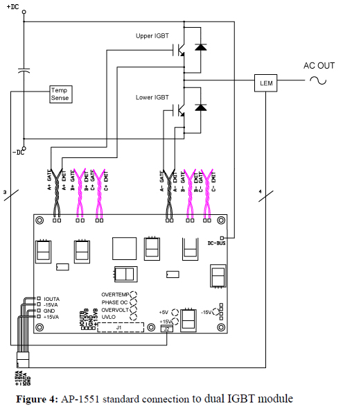
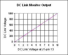
The positive of the DC link should be fed back to the GDB for monitoring and protection (see Figure 4). The reference for the DC link sense wire is the emitter of the lower IGBT (X-EMIT), which is also the ground of the DC link. This voltage is attenuated by a voltage divider (100:1) and transmitted across an optical barrier to provide an isolated, logic level representation of the DC link referenced to the ground of the GDB power supply. The attenuated voltage is available on pin 16 of J1 (600 volts on the DC link will result in 6.0 volts at pin 16) and is also used by the control logic to detect an over voltage condition (default threshold of 910 ± 10 VDC).
Temperature Sensing
The GDB temperature sense circuit uses an LM35 low cost, industry standard temperature sensor available in a TO-92 package. Unlike more expensive bi-metallic thermocouples, its output is immune to electrostatic and electromagnetic fields, which will undoubtedly be present in the system.
A 4-pin header on the board, J2, provides the necessary 15 volts and ground to power the LM35. The LM35 feeds back voltage proportional to temperature, which is scaled, buffered and available on pin 12 of J1.
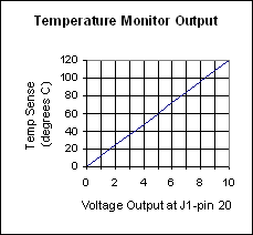
The scaling of the signal on pin 12 of J1 is 1V/12°C, where 0 volts is 0°C. The over temperature threshold is set on the GDB at 98 ± 2°C, which corresponds to 8.17 volts at pin 12. The threshold can be adjusted for a specific application.
Protection Features
The APS GDB is equipped with several protection features that will prevent catastrophic system failures. If any of the faults discussed below occur, all gate drive signals are latched off (user provided control signals are inhibited from reaching the gates) and the LED associated with the fault will light. The GDB will remain in a latched off state until both PWM+ and PWM- are held low for at least 8ms. When both control signals are held low for a minimum of 8ms, the latched fault will be reset. If the cause of the fault condition is removed, the control signals will be applied to the gates and the LED will be extinguished and the PWM+ and PWM- will be applied to the gates.
Reset Function
This 8ms reset feature is the reason that user generated dead time is neither required nor desired. If dead time of 8ms is supplied with the control signals, the unit will not properly latch off on a fault event and will continue to fire during faulted conditions. If an over current fault exists, the GDB will protect itself and the IGBTs on a pulse-by-pulse basis. However, the IGBTs may not be able to turn on into this condition indefinitely. Therefore, the control logic should heed the warning of the fault signals and inhibit the control signals when a fault is indicated and hold PWM+ and PWM- low until the system is checked out.
Over Current Protection
The first form of over current protection compares the sum of the currents from the Hall effect sensors to a predetermined threshold. When the threshold is exceeded, all gate drive signals are latched off within 2ms. They remain latched off until the fault condition is removed and PWM+ and PWM- are held low for at least 8ms.
The over current threshold should be set such that the voltage overshoot, due to the DC link inductance (see System Considerations), resulting at turn off does not reach destructive levels for the IGBTs being used.
The second form of over current protection on the GDB is used only with Powerex F-series IGBTs. When an over current condition is detected, the gate-emitter voltage is reduced to limit short circuit current. The APS BAP-1551 GDB senses this condition and performs a soft-turn-off of the IGBT conducting the excessive current. This form of over current is typically a shoot through with no load impedance to limit its magnitude. Therefore, a soft turn off is necessary to limit the voltage overshoot at turn off to a safe level. Upon detection of this condition the soft turn off is performed, all gate drive signals are latched off and the Phase OC (over current) LED is illuminated. The gate signals remain latched off until the fault condition is removed and PWM+ and PWM- are held low for at least 8ms.
When Powerex F-series IGBTs are not used, soft turn off current limiting can be implemented with standard desaturation detection. If the Vcesat of an IGBT exceeds a predetermined threshold while conducting, a soft turn off is executed. The same protection functions, annunciations and reset requirements apply with this form of short circuit protection.
Over Voltage Protection
The over voltage protection senses the DC link input and compares it to a predetermined threshold, 910 volts using 1200 volt devices and 450 volts using 600 volt Devices. When the threshold is exceeded for more than 1mS, the gate pulses are latched off 2ms later, and the over voltage LED is illuminated. The gate signals remain latched off until the fault condition is removed and all user provided control signals are held low for at least 8ms.
Over Temperature Protection
The over temperature protection uses the temperature sense input and compares it to a predetermined threshold, 98 ± 2 °C. When the threshold is exceeded for 1mS, the gate pulses are latched off 2ms later and the over temperature LED is illuminated. The gate signals remain latched off until the temperature sense input goes below 98°C and all user provided control signals are held low for at least 8ms.
Under Voltage Lock Out (UVLO)
The UVLO protection monitors the 15-volt logic supply, latches off the gate pulses and illuminates the UVLO LED if the 15-volt supply dips below 12 volts.
There is also an UVLO on each gate drive chip. When the power supply for a gate drive chip droops to a value that precludes the IGBT from being driven into saturation, the gate pulses are off until the fault condition is removed and PWM+ and PWM- are held low for at least 8ms.
Interfacing the BAP-1551 GDB to a Half-Bridge System
In order for the APS GDB to interface with a power stage, several connections need to be addressed:
Ribbon Cable connector J1 – A 16 pin ribbon cable connector is required to interface the GDB with the user provided controls. This connector can be purchased from 3M (part #3452-7600) along with strain relief (part #3448-3016) or an equivalent may be used. The pin assignments are detailed in Table 1. If the control logic already exists without a 16 pin header, terminal block to 16 pin header adapters are available.
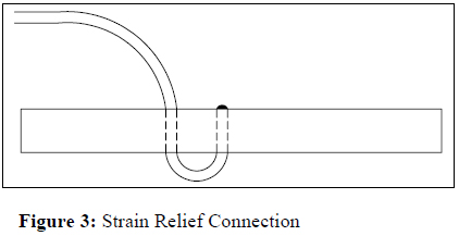
Gate Leads – The power stage should be packaged so that the gate leads are as short as possible. The gate leads should be a twisted pair of 22 AWG wires (approximately 2-3 turns per inch) of no more than one foot long, preferably 4-6 inches long. There are thru- holes next to the solder pads for each gate and emitter connection on the GDB. This can be used as a low cost, reliable strain relief by feeding the wire through the blank hole and then soldering the wire to the pad next to it. See Figure 3, below.
Standard gate lead lengths supplied are 3.5”. Longer or shorter leads are available upon request. Please see the form at the end of this Datasheet/Applications Note for additional information.
The interface with the IGBTs will be either a standard .110 fast-on or a ring terminal; whichever is applicable for the particular IGBT module you are planning to use. See the form at the end of this Datasheet/Application Note for additional information.
DC Link Connection – The DC link monitoring and over voltage protection are made possible by the DC link connection, which should be a single 22 AWG wire with a lug on the end to connect to the positive of the DC link. This wire’s interface with the GDB should be the same strain relief technique detailed in the gate lead section above.
Standard DC link lead length supplied is 3”. Longer or shorter leads are available upon request. Please see the form at the end of this Datasheet/Applications Note for additional information.
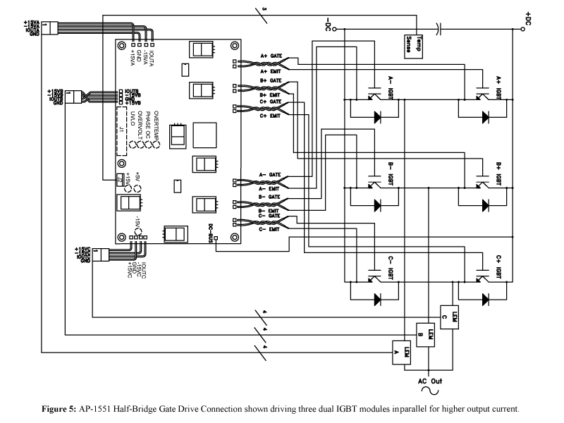
Current Sense Connection – When connected to one dual IGBT module, only a single four-wire connector is needed for the current transducer, as shown in Figure 4. When using two or three dual modules in parallel, the BAP-1551 has separate current sense connectors for each of the modules. A half bridge configuration using three dual modules in parallel is shown in Figure 5.
The connections are labeled on the GDB and are the required connections to interface with an HAS or HAC series produced by LEM (transducers made by other suppliers may require a different connection sequence and connector, refer to the suppliers’ datasheet). Wires and connector are supplied standard with the GDB conforming to the LEM connection pattern. To make the connections, 22AWG wire is used and employs the strain relief scheme shown in Figure 3. At the current sensor interface, LEM has a four-pin Molex connector part number 5045-04A. Supplied is an insulation displacement connector, Amp part number 640440-4 or equivalent.
A feature of the BAP-1551 GDB is its ability to drive up to three IGBT modules connected in parallel to generate higher currents. The BAP-1551 has additional connections to place as many as three dual IGBT modules in parallel. Shown in Figure 5 is the BAP-1551 GDB driving three dual IGBT modules. Note that the output of each module is connected together after the current transducer.
Standard current sense lead lengths supplied are 4”. Longer or shorter leads are available upon request. Please see the form at the end of this Datasheet/Applications Note for additional information.
System Considerations
There are many issues to consider when packaging a power stage including capacitor selection and configuration, routing of high current connections, heat sink size, and air or liquid cooling. These issues should be considered at the design stage and if not adequately addressed, a reliable power stage may never be realized.
Capacitors should be selected with ripple current capabilities sufficient for the particular application. For safety purposes, permanent bleeder resistors should be installed across the capacitors to ensure they are discharged when the power stage is turned off. The connection from the capacitors to the IGBTs should contain as little inductance as possible. Making this connection with a laminated bus is the most effective technique for minimizing bus inductance. A laminated bus uses flat sheet conductors separated by a thin insulator to force opposing currents to cancel magnetic fields thereby minimizing the inductance of the current path.
The low inductance will reduce voltage overshoots at turn off and will minimize if not eliminate the need for snubber capacitors. The voltage overshoot should be measured under controlled pulsed conditions at the over current threshold to be sure that IGBTs will not be destroyed due to over voltages.
There is stray capacitance from the electrical connections within the IGBT to its baseplate. The high dV/dTs inherent in IGBT based power stages will conduct current through this stray capacitance that can cause the heatsinks containing the IGBTs to float to dangerously high potentials. For this reason as well as to minimize noise coupling into the GDB, heatsinks should be earth grounded.
Heatsinks should be sized to dissipate the heat generated by the operation of the IGBTs. The total power loss (conduction losses and switching losses) of an IGBT power stage can be closely approximated using calculations based on IGBT and system parameters (APS applications engineers can assist with these calculations in certain situations). However, the calculated estimates should always be verified with empirical testing. Consult APS for heatsink and bus bar recommendations.
|
|||||||||||||||||||||||||||||||||||||||||||||||||||||||||||||||||
Notes:
|
|||||||||||||||||||||||||||||||||||||||||||||||||||||||||||||||||
|
|||||||||||||||||||||||||||||||||||||||||||||||||||||||||||||||||
|
|||||||||||||||||||||||||||||||||||||||||||||||||||||||||||||||||
|
|||||||||||||||||||||||||||||||||||||||||||||||||||||||||||||||||
|
|||||||||||||||||||||||||||||||||||||||||||||||||||||||||||||||||
|
|||||||||||||||||||||||||||||||||||||||||||||||||||||||||||||||||
|
|||||||||||||||||||||||||||||||||||||||||||||||||||||||||||||||||
|
Figure 11: Current scaling can be modified upon user’s request, contact APS. |
|||||||||||||||||||||||||||||||||||||||||||||||||||||||||||||||||


